Rs232_syscon
User’s Guide
version 1.00
Writen By John Clayton
Scottsdale, AZ
2001.8.13
Purpose:
This document describes some of the design features of
"rs232_syscon.v" (a softcore written in Verilog.) It is intended to facilitate new users in understanding what is available in the core, and how to use it. Also, the Verilog code itself is replete with comments, so that additional insights into the operation of this core can be gained by reviewing the code.Release Log
V1.00 Aug. 13, 2001
1.Introduction
The name "rs232_syscon" comes from rs232 (serial communication standard) and an abbreviated contraction of "system controller." The core actually uses LVTTL levels for the serial connection, and the user is responsible for providing level shifting translators to achieve rs232 standard voltage levels.
The rs232_syscon project was conceived on May 30, 2001. It’s purpose was to develop a "serial-port-to-bus-interface" core suitable for debugging some other ps2_mouse and ps2_keyboard interface cores which were under development at the time… Those other cores were quickly completed, but the actual development of rs232_syscon was more complicated than originally thought, and it ended up taking longer to complete. Luckily, as its development progressed, rs232_syscon became simpler instead of more complicated.
After many hours of debugging and coding, the rs232_syscon core is now functional, and it has been successfully used to test out memory blocks and register blocks as part of a "system on a chip" (SOC) design effort.
This document describes the following:
In reality, rs232_syscon is a simple core to use – once it is connected to the data and address buses and the BAUD rate is adjusted, it can be used immediately. It does not contain any architecture specific blocks, so it easily ports to different FPGA and even ASIC platforms.
2. rs232_syscon connections
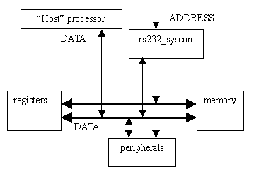
2.1 Block diagram
A top-level block diagram of rs232_syscon being used in a system is shown in figure2.1 below.
Since the address bus is not bidirectional, it is an output from the host processor, and also an output from rs232_syscon. In order to select which device gets to drive the address bus, a multiplexer is implemented inside of rs232_syscon. This introduces some additional delay in the address bus, which is considered an acceptable tradeoff in exchange for the enhanced debugging capability of rs232_syscon. Besides, when debugging is completed, the mux can be removed (or "hard wired" by a parameter at compile time, which will also result in the eventual removal of the mux because of optimization in the synthesis and routing tools…)
figure 2.1
The data bus is implemented as a tri-state bus, so that it can be bi-directional without requiring the use of multiplexers. The designers of rs232_syscon were aware that the Wishbone standard seems to encourage a split data bus (dat_i for input data and dat_o for output data) but found that the Wishbone standard also allows for tri-state connections (See Wishbone spec. page 66). The tri-state data bus was chosen in order to reduce the number of internal interconnects needed to implement the bus. If a tri-state bus is unacceptable for your application, the rs232_syscon block can be easily modified to add "dat_i" and "dat_o" ports in place of the existing "dat_io" port, and the tri-state buffering can be removed. This is not difficult for a Verilog programmer to accomplish, and it does not require any major functional modifications to the rs232_syscon block. The same handshaking structure that is used for address bus multiplexing ("master_br_o" and "master_bg_i") could also be used to control the data bus multiplexers.
The handshaking scheme in rs232_syscon allows the rs232_syscon to request access to the bus from the normal bus master. This is accomplished through the "master_br_o" and "master_bg_i" pins. Once the bus request (br) is detected at the normal bus master, it should finish the current operation, and then assert and keep asserting "master_bg" to rs232_syscon. As long as the bus grant (bg) line is asserted into rs232_syscon, then rs232_syscon will know that it has control of the bus. Also, when rs232_syscon finishes generating its bus cycles, it does not check or wait for the bus grant line to be deasserted. Therefore, those who wish to test peripherals, memory or registers without another master on the bus, can simply tie "master_bg_i" high, or just connect it to the rs232_syscon’s "master_br_o" and forget about that handshaking interface.
The bus cycles generated by rs232_syscon are one clock long. The clock which is used with rs232_syscon can vary up to the maximum speed allowed by the architecture in which it is being used. In a Xilinx SpartanII device (XC2S200) it synthesized with a maximum clock speed of around 45 MHz, although most of the testing was done at around 25 MHz. The length of each bus cycle is extended until the "ack_i" signal is received by rs232_syscon. If the watchdog timer expires before "ack_i" is received, then a bus error message is generated for the user. Similarly, if the "err_i" signal is received, then a bus error message is generated for the user.
2.2 Parameter listing
|
Parameter Name |
Range |
Function |
|
ADR_DIGITS_PP |
1..? |
Width of address bus in nibbles (4 => 16bits, 8 => 32 bits) |
|
DAT_DIGITS_PP |
1..? |
Width of data bus in nibbles |
|
QTY_DIGITS_PP |
1..? |
Width of qty counter in nibbles |
|
CMD_BUFFER_SIZE_PP |
16/32/64 |
Characters in command buffer (drives logic size significantly) |
|
CMD_PTR_BITS_PP |
4/5/6 |
Width of pointer to command buff. |
|
WATCHDOG_TIMER_VALUE_PP |
1..? |
Number of clocks before timer expires |
|
WATCHDOG_TIMER_BITS_PP |
1..? |
Number of bits in watchdog timer |
|
RD_FIELDS_PP |
1..? |
Number of columns shown for read |
|
RD_FIELD_COUNT_BITS_PP |
1..? |
Number of bits in rd_field_count |
|
RD_DIGIT_COUNT_BITS_PP |
1..? |
Number of bits in rd_digit_count |
The defaults for these parameters are given in the Verilog code. The settings are related to each other, as explained in the code also. For instance, if the watchdog_timer is set to expire after 32000 clocks, then there must be 15 bits in the watchdog timer, so that parameter must be set accordingly.
2.3 Pinout description (port listing)
|
Name |
Size |
Function |
|
clk_i |
1 |
Clock input |
|
reset_i |
1 |
Resets rs232_syscon unit |
|
master_bg_i |
1 |
Grants bus to rs232_syscon |
|
ack_i |
1 |
Wishbone bus cycle acknowledge |
|
err_i |
1 |
Wishbone bus cycle error |
|
rs232_rxd_i |
1 |
rs232 serial port data input |
|
dat_io |
parameter |
data bus (tri-state) |
|
rst_o |
1 |
Wishbone reset output |
|
master_br_o |
1 |
Requests bus for rs232_syscon |
|
stb_o |
1 |
Wishbone strobe output |
|
cyc_o |
1 |
Wishbone cycle output (wired to stb_o in this version) |
|
adr_o |
parameter |
address bus |
|
we_o |
1 |
Wishbone write enable output |
|
rs232_txd_o |
1 |
rs232 serial port data output |
3.0 Command syntax
The commands for rs232_syscon are very simple. There are three of them – read, write and initialize (reset). The spacing of the characters in the command does not matter – spaces and tabs are considered "whitespace." The enter key terminates the command, and begins the process of parsing and executing the command. All numbers are given in hexadecimal. Hexadecimal numbers are printed using capitalized letters, but case does not matter when entering commands.
The command syntax is as follows, where "aaaa" refers to address, "dddd" refers to data, and "qq" refers to quantity.
Write command: w aaaa dddd qq
Read command: r aaaa qq
Initialize command: i
The command character (w,r,i) is the only required part of the command. If the data field is left out, then the previous value is assumed. If the address field is left out, then the previous value is assumed. Default values for address and data are both zero. An exception to this rule is the quantity field (qq), which does NOT assume the previous value. Instead, if quantity is not specified, it assumes the value "1," which is generally what the user intends for a command that does not specify quantity.
When entering quantity explicitly, the value zero is allowed. In that case, the command will do nothing. No bus cycles will be generated. For quantity values greater than one, the address field is automatically incremented during the subsequent iterations of the command loop. However, the data remains the same.
Extra fields can be entered after the "i" command, but they will not have any effect.
3.1 Numerical Field length
Using too few characters for a given numerical field will not produce an error – for instance, if the address/data buses are 16-bits wide, and you wish to enter the value 0005 into address 0017, it is sufficient to say:
w 17 5 [enter]
The leading zeros are assumed by the command parser. Similarly, if too many digits are used, only the appropriate number of digits (the right hand ones) are used. For instance, consider the command:
w 5434540017 66677560005 [enter]
This would have the same effect as the first example, because only the four digits on the right side are used (0017 and 0005 respectively).
backspace is allowed, and the cursor will move inside the rs232 terminal to indicate that a character has been "deleted" from the command line, even if the character itself still shows up on the terminal screen.
The maximum number of characters that can be entered on the command line is determined by the size of the command buffer (a parameter setting.) When that length is reached, if the [enter] key has not yet been pressed, a ‘?’ message will be returned, indicating a parsing error.
3.1 Parsing errors
The different responses which can be generated from rs232_syscon are listed here:
|
Response |
Meaning |
|
OK |
The command was parsed and executed without error |
|
? |
Line length exceeded |
|
A? |
Address field parsing error |
|
D? |
Data field parsing error |
|
Q? |
Quantity field parsing error |
|
! |
"err_i" or else watchdog timeout before "ack_i" |
|
B! |
Watchdog timeout before bus grant |
The watchdog timer is used twice during the execution of a command. The first time it is used to determine if there was a timeout for obtaining the bus, and the second time it is used to determine if the bus cycle timed out, with no "ack_i" response. Therefore, a slow master together with a slow peripheral could conceivably use almost twice the time period of the watchdog timer, in order to complete the execution of the command.
3.2 Initial power up
The initial power up of rs232_syscon produces the following stream of characters which are sent to the terminal:
0123456789ABCDEF
-> [cursor]
This initial stream of characters can be used to verify that your terminal is set to the correct BAUD rate.
Also, no activity is generated to reset the peripherals on the bus upon initial power up. Therefore, in order to reset the peripherals on the bus, an explicit "i" command must be issued. Resetting the rs232_syscon unit will return all quantities to zero, but it will not generate the "rst_o" signal which is generated by the "i" command.
3.3 Actual session logfile
Here is the text from part of a debugging session using the rs232_syscon module (none of the bus error responses are shown here):
<Session begins>
0123456789ABCDEF
-> w 1 55 1
OK
-> w 1 5a
OK
-> w 4 4c
OK
-> w 2 140
OK
-> w 3 100
OK
-> w 4 5c
OK
-> w 4 6c
OK
-> w 2 150
OK
-> w 3 f8
OK
-> w 3 f0
OK
-> w 3 f8
OK
-> w 3 f7
OK
-> w 3 48
OK
-> r 3
0003 : 0048 OK
-> r 0 8
0000 : 0000 005A 0150 0048 006C 0000 0000 0000
OK
-> r 0 10
0000 : 0000 005A 0150 0048 006C 0000 0000 0000
0008 : 0000 005A 0150 0048 006C 0000 0000 0000
OK
-> r 0 20
0000 : 0000 005A 0150 0048 006C 0000 0000 0000
0008 : 0000 005A 0150 0048 006C 0000 0000 0000
0010 : FFFF FFFF FFFF FFFF FFFF FFFF FFFF FFFF
0018 : FFFF FFFF FFFF FFFF FFFF FFFF FFFF FFFF
OK
-> w 3 58
OK
-> w 3 68
OK
-> r 0 10
0000 : 0000 0068 0068 0068 0068 0068 0068 0068
0008 : 0000 0068 0068 0068 0068 0068 0068 0068
OK
-> w 3 58 1
OK
-> w 4 68 1
OK
-> r 0 10
0000 : 0000 0068 0068 0058 0068 0068 0068 0068
0008 : 0000 0068 0068 0058 0068 0068 0068 0068
OK
-> w 4 6c 1
OK
-> w 4 7c 1
OK
-> w 1 f4 1
OK
-> r 0 8
0000 : 0000 00F4 0068 0058 007C 0068 0068 0068
OK
<session ends>
4.0 BAUD rate generators
The BAUD rate used in rs232_syscon is determined by a in internal signal called "serial_clk_16x." This signal is not actually implemented on a clock net. Instead, it is a clock enable. Using a clock enable for this slow signal is perfectly acceptable in most cases, and it has the advantage that it does not use an additional dedicated clock resource on the target FPGA.
As indicated by the name, the signal occurs at 16 times the desired BAUD clock rate. For 115,200 BAUD it is a high pulse which occurs for one single "clk_i" clock period, at a rate of 16*115200 = 1.8432 MHz.
This clock enable pulse is derived from a higher frequency clock on your board, by a small DDS (Direct Digital Synthesizer.) It sounds more complicated than it is. This DDS does not produce a sine-wave output, it merely produces a single pulse at the desired rate. You can use different modules from "serial.v" in order to do this. The "clock_gen_select" allows you to use a lookup table of DDS phase increment values (which are directly related to the output frequency) so that the BAUD rate can be changed easily between common values.
On the other hand, you could choose to use the "clk_gen" module from serial.v in order to generate a single, fixed BAUD clock.
You will almost certainly need to re-calculate the DDS "frequency" inputs for use with your board, since you will undoubtedly be using some clock other than the 49.152 MHz which I chose to use.
However, the nature of the DDS circuit is such that you can most likely find a way to make it work without having to change your system clock frequency. Almost anything can be made to work. Some frequency error is tolerable in the BAUD clocks, and by making the DDS bigger then more and more resolution is obtained until it works for your frequency... Detailed instructions are given in "serial.v" on how to recalculate new values for use in your application. Or you can simply get a different clock!