Description
MIPS-lite is a "clean room" VHDL implementation of a MIPS CPU. It supports a simplified MIPS III+ instruction set with a two-stage pipeline. Only User Mode instructions are supported.
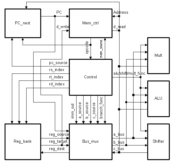
Block Diagram
As an example, an ADD instruction would take the following steps:
The CPU is implemented as a two-stage pipeline with step #1 in the
first stage and steps #2-8 occurring the second stage.
Each instruction takes one clock cycle, except memory accesses,
which take two clock cycles, and multiplication and division, which
can be accessed in 32 clock cycles.
There are several control lines not shown in the diagram.
A pause (wait-state) line will cause the pipeline to pause
if the multiplication results are accessed before the
multiplication is complete.
Supporting Documentation
The implementation is based on information found in:
The tools used include VHDL Synopsys, ModelTech, and the Microsoft MIPS C compiler.
Registers
All of the registers are clocked by the single master clock. The registers used in the design are grouped by entity and listed below:
     mem_ctrl
     ===========================================
     |    Register Name    |   Type    | Width |
     ===========================================
     | next_opcode_reg_reg | Flip-flop |  32   |
     |   opcode_reg_reg    | Flip-flop |  32   |
     |   setup_done_reg    | Flip-flop |   1   |
     ===========================================

     mult
     ===========================================
     |    Register Name    |   Type    | Width |
     ===========================================
     |   answer_reg_reg    | Flip-flop |  32   |
     |    count_reg_reg    | Flip-flop |   6   |
     |   do_div_reg_reg    | Flip-flop |   1   |
     |  do_signed_reg_reg  | Flip-flop |   1   |
     |      reg_a_reg      | Flip-flop |  32   |
     |      reg_b_reg      | Flip-flop |  64   |
     ===========================================

     pc_next
     ===========================================
     |    Register Name    |   Type    | Width |
     ===========================================
     |     pc_reg_reg      | Flip-flop |  30   |
     ===========================================

     reg_bank
     ===========================================
     |    Register Name    |   Type    | Width |
     ===========================================
     |      reg01_reg      | Flip-flop |  32   |
     |      reg02_reg      | Flip-flop |  32   |
     |      reg03_reg      | Flip-flop |  32   |
     |      reg04_reg      | Flip-flop |  32   |
     |      reg05_reg      | Flip-flop |  32   |
     |      reg06_reg      | Flip-flop |  32   |
     |      reg07_reg      | Flip-flop |  32   |
     |      reg08_reg      | Flip-flop |  32   |
     |      reg09_reg      | Flip-flop |  32   |
     |      reg10_reg      | Flip-flop |  32   |
     |      reg11_reg      | Flip-flop |  32   |
     |      reg12_reg      | Flip-flop |  32   |
     |      reg13_reg      | Flip-flop |  32   |
     |      reg14_reg      | Flip-flop |  32   |
     |      reg15_reg      | Flip-flop |  32   |
     |      reg16_reg      | Flip-flop |  32   |
     |      reg17_reg      | Flip-flop |  32   |
     |      reg18_reg      | Flip-flop |  32   |
     |      reg19_reg      | Flip-flop |  32   |
     |      reg20_reg      | Flip-flop |  32   |
     |      reg21_reg      | Flip-flop |  32   |
     |      reg22_reg      | Flip-flop |  32   |
     |      reg23_reg      | Flip-flop |  32   |
     |      reg24_reg      | Flip-flop |  32   |
     |      reg25_reg      | Flip-flop |  32   |
     |      reg26_reg      | Flip-flop |  32   |
     |      reg27_reg      | Flip-flop |  32   |
     |      reg28_reg      | Flip-flop |  32   |
     |      reg29_reg      | Flip-flop |  32   |
     |      reg30_reg      | Flip-flop |  32   |
     |      reg31_reg      | Flip-flop |  32   |
     |     reg_epc_reg     | Flip-flop |  32   |
     |   reg_status_reg    | Flip-flop |   1   |
     ===========================================
Preliminary Synthesis
The CPU core was synthesized for 0.13 um line widths with a predicted
area less than 0.2 millimeters squared. The predicted maximum
latency was less than 6 ns for a maximum clock speed of 150 MHz.
A preliminary synthesis yields the following cells and die area.
I think that optimization caused the mips_cpu entity
to be smaller than the sum of its
components.
If one assumes that a standard cell is composed of three gates,
then this is approximately a 20K gate design. [Is this correct??]
It is interesting to note that the register bank requires over 60% of the area.
     Block    ports   nets  cells cell_area   ~%   delay(ns)
     ------   -----   ----  ----- ---------  ---   ---------
     alu        101    919    850      7503   12        1.11
     bus_mux    283    672    486      4906    8        0.35
     control     93    296    263      2250    4        0.29
     mem_ctrl   271    455    318      3299    5        0.95
     mult       101   1111   1043      9342   15        0.72 ??
     pc_next     94    277    215      1756    3        0.15
     reg_bank   116   2650   2599     39477   62        1.02
     shifter     71    423    384      3026    5        1.51
     mips_cpu   201    555     45     63888  100        5.61

     total     1331   7358   6203
List of Files
| FILE | PURPOSE |
| makefile | Makefile for the HP workstation for Synopsys |
| code.txt | Input opcodes for the test bench -- test.exe "converted" |
| alu.vhd | Arithmetic Logic Unit |
| bus_mux.vhd | BUS Multiplex Unit |
| control.vhd | Opcode Decoder |
| mem_ctrl.vhd | Memory Controller |
| mips_cpu.vhd | Top Level VHDL for MIPS CPU |
| mips_pack.vhd | Constants and Functions Package |
| mult.vhd | Multiplication and Division Unit |
| pc_next.vhd | Program Counter Unit |
| ram.vhd | RAM for the Test Bench |
| reg_bank.vhd | Register Bank for 32, 32-bit Registers |
| shifter.vhd | Shifter Unit |
| tbench.vhd | Test Bench that uses mips_vpu.vhd and ram.vhd |
| makefile | Makefile for the PC for creating "code.txt" |
| convert.c | Converts test.exe to code.txt |
| mips.c | Simulates a MIPS CPU in software |
| test.c | Test program (opcodes) for the MIPS CPU |
| output.txt | Output from the test bench |
| index.shtml | This help file |
| cpu.gif | Block Diagram |
Download Files
Use CVS to download the files in the "mips" project. To run a CGI script to run CVS to get all the files click here.
Convert
The program "convert" changes the file "test.exe" into the HEX file "code.txt". The opcodes in "test.exe" are changed to Big Endian. All absolute jumps are changed to relative jumps. The first opcode is also changed to set up the stack pointer.
Big/Little Endian
The MIPS CPU operates in Big Endian mode by default. To operate in Little Endian mode, change "little_endian" from "00" to "11" in the file mem_ctrl.vhd.
Legal Notice
MIPS is a registered trademark of MIPS Technologies, Inc.
If you use this core you are responsible for all legal issues.
This "clean room" implementation of a MIPS CPU does not negate
MIPS Technologies, Inc. of their trademark, copyrights, or patents....
Free for commercial and non-commercial use as long as the author and
warning notices are maintained.
This software is provided by Steve Rhoads "as is" and
any express or implied warranties, including, but not limited to, the
implied warranties of merchantability and fitness for a particular purpose
are disclaimed. In no event shall the author or contributors be liable
for any direct, indirect, incidental, special, exemplary, or consequential
damages (including, but not limited to, procurement of substitute goods
or services; loss of use, data, or profits; or business interruption)
however caused and on any theory of liability, whether in contract, strict
liability, or tort (including negligence or otherwise) arising in any way
out of the use of this software, even if advised of the possibility of
such damage.
Bus Interface
   port(clk         : in std_logic;
        reset_in    : in std_logic;
        intr_in     : in std_logic;  --interrupt line

        --memory access buses
        mem_address : out std_logic_vector(31 downto 0);
        mem_data_w  : out std_logic_vector(31 downto 0); --avoided tri-state
        mem_data_r  : in std_logic_vector(31 downto 0);
        mem_sel     : out std_logic_vector(3 downto 0);	 --byte lines
        mem_write   : out std_logic;
        mem_pause   : in std_logic
        );
Current Status
Maintainer
Mailing-list